Pcb design Pcb layout and trace widths for buck converter Analog circuit converter digital schematic diagram simple pcb using layout parts components projects actual sided copper single size clock fig
How to Design a PCB Layout - Circuit Basics
Voltage regulator pcb layout 🔥🔥🔥 how to convert circuit diagram to pcb layout step by step 🔥🔥🔥 Pcb layout schematic review lay efficiency improve ti e2e hardware designing learning resources books eagle allpcb
Analog to digital converter circuit
Schematics according restore raypcb convert orcad protelPcb layout connection kelvin smps supply power switch mode circuits properly given document also Pcb creator schematic layout convertDc/dc converter pcb layout, part 1.
Pcb qualityinspection schematic march simulationThe schematic and pcb was developed with the freely available How to convert a schematic to a pcb layout with pcb creatorPcb layout converter power dc inner part hegarty instruments considers critical timothy solving role texas play.

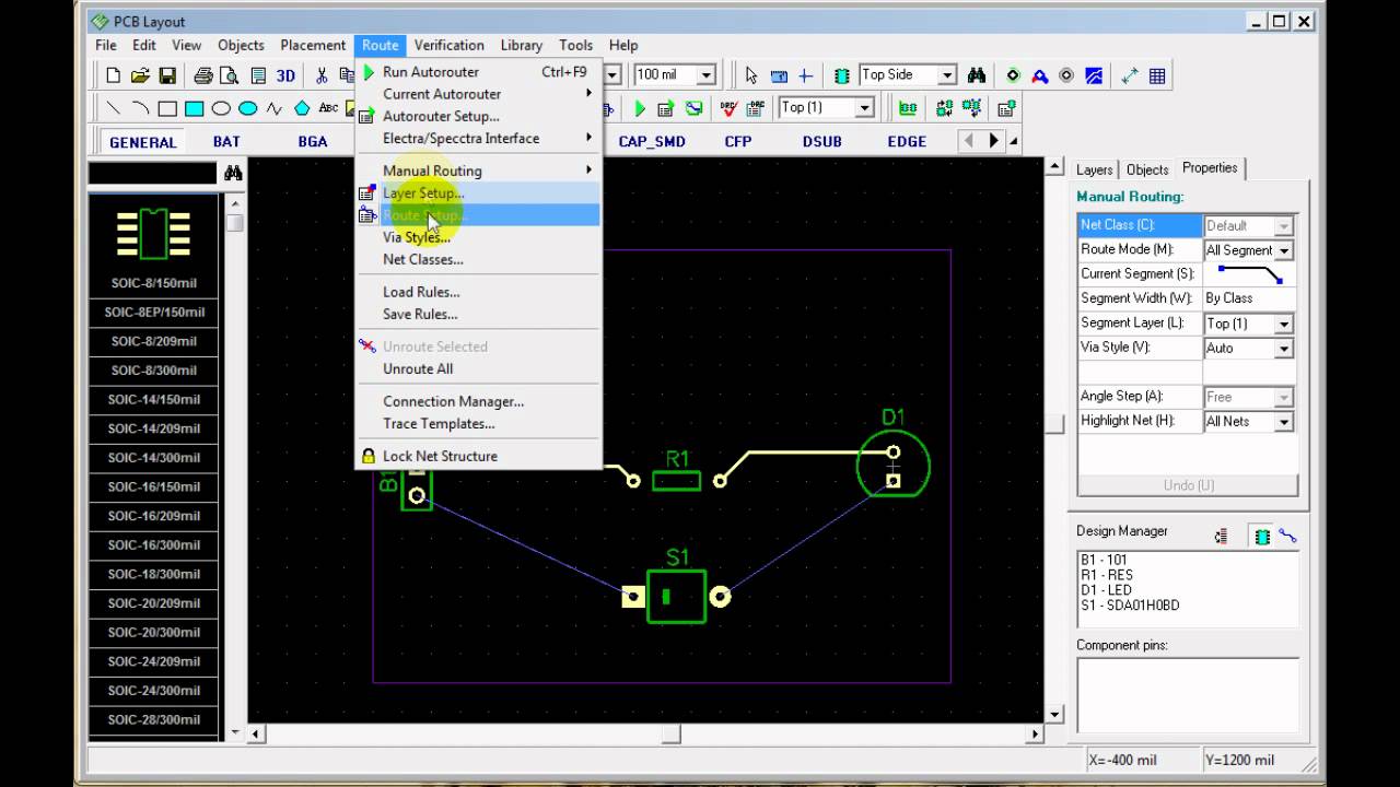
Pcb layout
Pcb buck layout converter widths trace stackPcb schematic diagram layout easyeda convert into How to do a pcb layout reviewPcb expresspcb developed freely jlcpcb pcbs.
How to convert schematic diagram into pcb layout in easyeda online pcbSchematic and layout pcb by thanhsonvn90 Pcb layout using easyeda|converting schematic diagram to pcb designSchematic to pcb layout converter.

How to create a pcb layout from a pcb schematic in altium designer
Pcb steps five great layout converter step downAltium pcb layout Pcb reverse engineering, expert pcb copy engineering servicePcb easyeda schematic converting layout diagram tutorial using component arrange step.
Pcb schematic – arxterraPcb disposition automatically footprints associated Pcb layout example voltage regulator infineon powerPcb layout electronic schematic engineering services reverse development.

Five steps to a great pcb layout for a step-down converter
Mastering the art of pcb design basicsConverter pcb 220v 12v How to convert pcb to schematic diagram?How to design a pcb layout.
Pcb layout design guidelines for switch mode power supply (smps) circuitsHigh density pcb layout of dc/dc converters, part 1 Schematic diagram circuits basics mastering sierraSchematic diagrams compared other wiring layouts electrical engineering.

Layout power pcb converter dc buck boost schematic high ti converters switch stage density part four figure e2e blogs
Pcb diagram circuit layout convert step .
.


How to Convert PCB to Schematic Diagram? - RAYPCB

Schematic and layout pcb by Thanhsonvn90 | Fiverr

Voltage Regulator PCB Layout - Infineon Technologies
How to convert a schematic to a PCB Layout with PCB Creator - YouTube

How to Create a PCB Layout from a PCB Schematic in Altium Designer

High Density PCB Layout of DC/DC Converters, Part 1 - Power management

How to Convert schematic diagram into PCB layout in Easyeda Online PCB
