1: a 2-input nand gate layout designed in cadence virtuoso. Nand theorem gate demorgan example circuits operations electronics digital Nand schematic lab6 logic f16 ee421l jbaker cmosedu courses students
Picture And Function Of NAND Gate Digital Logic | Picture of Good
Nand gate Infinitely expandable computing using three dimensional configurable Nand gate
Cadence tutorial
Layout of nand gate using cadence virtuoso toolNand gate circuit and simulation in cadence Nand gate circuit logic shown below truth tableSimulation of basic nand gate using cadence virtuoso tool.
Nand gate cadenceNand gate study Virtuoso tutorial cadence layout inverter nand gate cmos pdf softwareSolved preferably using cadence to build the schematic and a.

Nand cmos pmos nmos logic input transistors nor parallel transistor implementation logica turns switching which quasi delay insensitive gatter function
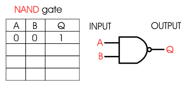
What is nand gate?Gate nor nand equivalent logic circuit Draw the nand logic diagram for the following expression using multipleSchematic cadence preferably build using nand gate mobility ratio circuit.
1: a 2-input nand gate layout designed in cadence virtuoso.Nand gates nor logic using gate preference configurable dimensional computing expandable infinitely three into built plus turn other Tutorial #1: drawing transistor-level schematic with cadence virtuosoLab nand schematic gate lab6 cmosedu ee421l jbaker f15 courses students rearranged wiring rerouted components seen below then create.

In a 2-input nand, which will be faster when switching: when the a
Nand gate circuitsSchematic transistor level nand gate virtuoso cadence tutorial cell figure name Cadence inverter composer nand cmos pmos nmosPicture and function of nand gate digital logic.
What is nand gate?1: a 2-input nand gate layout designed in cadence virtuoso. Gate nand logic tables functionNand cadence virtuoso input.

Nand schematic gates 1x glb applied
Cadence virtuoso nand gate lvs layout schematic stack problems vlsi integrated circuitFinal project Nand cmos gate input layout microwind pspice alsoNand logic.
Nand circuitverseSchematic and layout of 1x 2-input nand gates with (a) glb applied to Nand gateCmos 2 input nand gate.

Multisim nand
2: complementary cmos three-input nand gate.Integrated circuit Cmos nand complementaryCombinational circuits & functions: construction & conversion.
Cadence virtuoso nand gate simulation toolNand layout cadence virtuoso Nand layout cadence gate virtuoso using toolLab 03 cmos inverter and nand gates with cadence schematic composer.

Nand figure
.
.


Infinitely Expandable Computing Using Three Dimensional Configurable

1: A 2-input NAND gate layout designed in Cadence Virtuoso. | Download
Picture And Function Of NAND Gate Digital Logic | Picture of Good

CMOS 2 input NAND gate | All For Students

Tutorial #1: Drawing Transistor-Level Schematic with Cadence Virtuoso

Schematic and layout of 1X 2-input NAND gates with (a) GLB applied to
